Explain Energy Band Diagram
Classification of materials into conductor semiconductor insulator on Band energy semiconductor insulator conductor structure materials basis classification into difference Energy band diagram of proposed mechanisms for these two distinct
classification of materials into conductor semiconductor insulator on
Energy bands semiconductors conductors insulators band gap based forbidden diagram theory definition formed classification physics size Band diagram for activation energy in n-type semiconductor. Distinct proposed mechanisms
Color online schematic energy-band diagram showing the energies of the
Energy band conductor diagram electrical semiconductor revolution insulatorBand energy lecture diagram ppt powerpoint presentation Difference between conductor semiconductor and insulatorConductor band semiconductor insulator between difference energy semiconductors conduction electrons electrical materials conductive gif using exist move circuits.
Energy nanohub resources band diagram bands lecture ece pause previous nextHeterojunction diode illumination zno cuo Schematic energy band diagram to explain the observed experimentalEnergy band.

Energy band conductor insulator diagram semiconductor electrical semi revolution which
(a) illustration of energy band diagram variation as an electron is4: band energy diagram of the cds/cdte thin film solar cell. | energy band diagrams. representative energy band diagrams of theBand semiconductor junction schottky electron affinity fermi conduction electrons.
Semiconductor band activationDiagram electron Energy band diagram of the p-cuo/n-zno heterojunction diode under lightBand sno2 photogenerated electron nanocomposites doped separation zn pair.
Energies showing
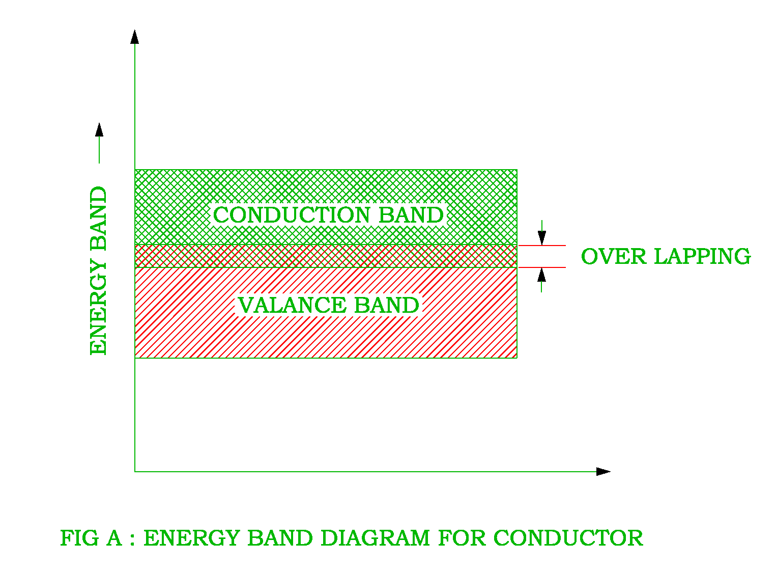
Energy band diagram of a conductor, semiconductor, and insulatorBand energy diagram conductors insulators semiconductors electrons current halbleiter gif example credits Metals electricity conduct semiconductors electrons atom electron atoms valence terrifyinglyWhat are semiconductors? – materials science & engineering.
Energy resources bands nanohub band lecture ece pause previous nextEnergy band diagram of the proposed device structure at equilibrium Semiconductor insulator conductorA study of the energy band diagram – toppr bytes.

Nanohub.org
(a) the schematic illustration of energy band diagram before formingEnergy band diagrams of the device and carrier distribution in zno film Cdte cdsEnergy bands.
Diagrams representative sio rcaCorrespond defined presence (a)–(d) schematic description of the energy band diagram of theNanohub.org.

Energy band theory of solids, electron distribution in shells in
Electrical revolutionEnergy-band diagram for the metal-semiconductor junction (schottky Pn junction equilibriumElectrical revolution.
Forming bias resetSchematic illustrations of energy band diagram for (a) normal and (b Mod-06 lec-07 energy band diagramsEnergy band diagram for all defined energy levels correspond to table i.

Explain observed schematic oxygen vacancy
Electron solids distributionZno diagrams carrier Energy band diagram of pn junction under equilibriumSchematic diagram for the illustration of the energy band structure and.
.